The chassis is open for explanation. Never open the chassis as there is a high voltage part inside.
Copyright(C) 2022 Shoichi Yoshimoto
The chassis is open for explanation. Never open the chassis as there is
a high voltage part inside.
Model10 uses a fully differential circuit to obtain high-quality balanced
and unbalanced outputs at the same time.
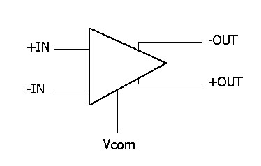
A fully differential amplifier is an amplifier that has 5 terminals: + IN and -IN input terminals, + OUT and -OUT output terminals, and Vcom terminal.
The difference between + IN and -IN is amplified and output between + OUT
and -OUT.
Vcom sets the midpoint voltage between + OUT and -OUT.
For headphone amplifiers, Vcom is 0V (ground).
Vcom keeps + OUT and -OUT at 0V when no signal is input (low DC offset).
At the time of signal input, a balanced voltage is output to + OUT and
-OUT.
One channel of Model10 consists of 4 differential amplification stages
and 2 SEPP output output stages.
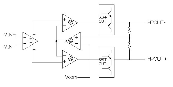
'1' is a first-stage differential amplifier with 2N7002DW dual MOSFET.
The input signal is differentially amplified and sent to the positive driver
stage '3' and the negative driver stage '2'.
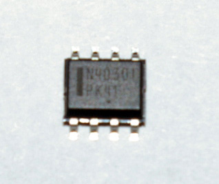
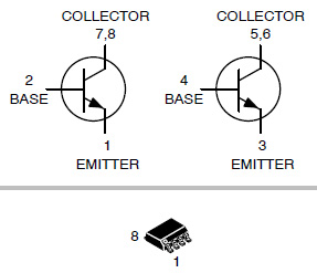
'2' and '3' are driver stage differential amplifiers with NSS40300MDR2G
dual PNP Tr.
Positive and negative signals are amplified to a large amplitude and sent to the SEPP stage by dual Tr.
Headphones are driven with low impedance by the SEPP stage.
'4' is a common mode feedback differential amplifier by NSS40301MDR2G dual NPN Tr.
Compare Vcom with the output midpoint and create an error signal to maintain
the output potential and the balance between the outputs . The error signal
is sent to the negative input of the driver stage and cancels the error
(common mode) that occurs in the output.
The figure below is a circuit diagram for one channel of Model10.
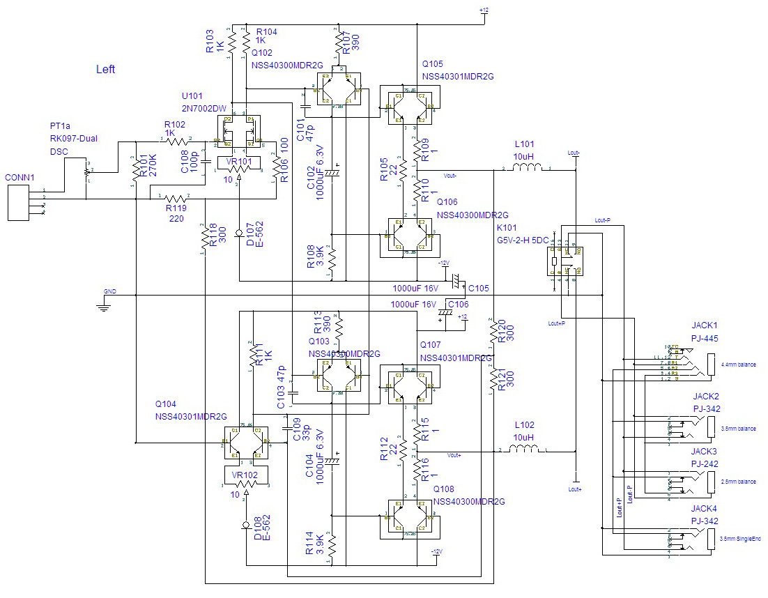
Model10 uses dual elements in all stages.
 |
 |
 |
 |
 |
Since Model10 is a balanced output with a stereo configuration, it has four SEPP output stages.
The idling currents of the four SEPP output stages must be set and maintained
the same.
In order to improve productivity and reliability, the idling current of
the SEPP output stage has been noadjusted and stabilized.
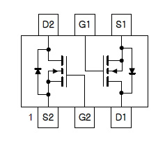
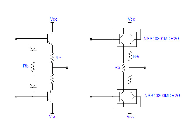
The left of the figure below is the general SEPP output stage, and the
right of the figure below is the SEPP output stage of Model10 using dual
Tr.
In a general SEPP output stage, it is necessary to adjust Rb as a variable
resistor or select a temperature compensation diode in order to achieve
the target idling current value.
Model10 gained the following advantages by replacing the temperature compensation
diode with a dual Tr diode connection.
・Perfect temperature compensation with adjacent diodes and Trs in the
same silicon chip.
・Since the diode and Tr have the same process and the same manufacturing
conditions, the Vbe characteristics are the same.
As a result, the target idling current value can be stably obtained even if Rb is used as a fixed resistor.
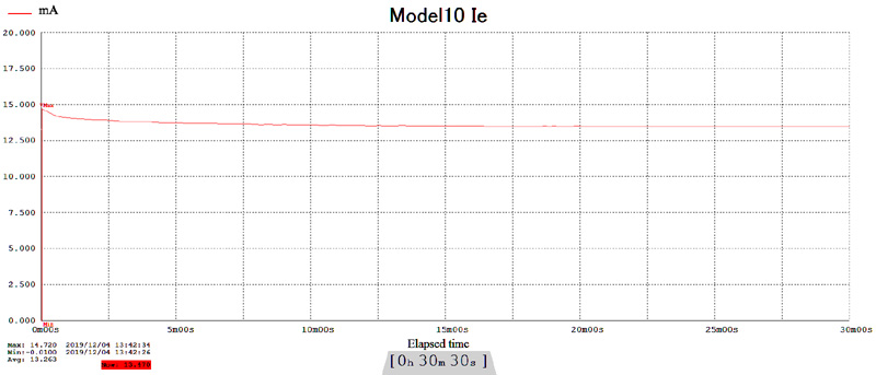
The figure below shows the idling current measurement results from the
time the power is turned on until 30 minutes have passed.
Immediately after the power is turned on, the idling current is 15mA, but
after 5 minutes it stabilizes at 13.5mA.
Since Model10 is a DC amplifier, a protection circuit is provided to protect the headphones from the following events.
Headphones are more vulnerable than speakers, so highly sensitive DC output
detection is required.
Furthermore, since Model10 is a balanced output stereo amplifier, it is
necessary to detect DC output at four points.
The protection circuit operates the relay under the following conditions
to disconnect the headphones.
If these protection operations are realized by a conventional circuit, it will be large-scale.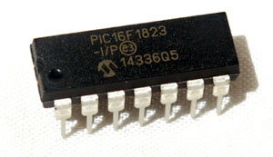
Therefore, it is realized simply by using the PIC microcomputer PIC16F1823.
PIC16F1823 is a microcomputer equipped with high functionality such as
7ch 10Bit AD input in a 14pin DIP package.
The 10Bit AD input monitors the headphone output for 4 channels and the
voltage of the power supply.
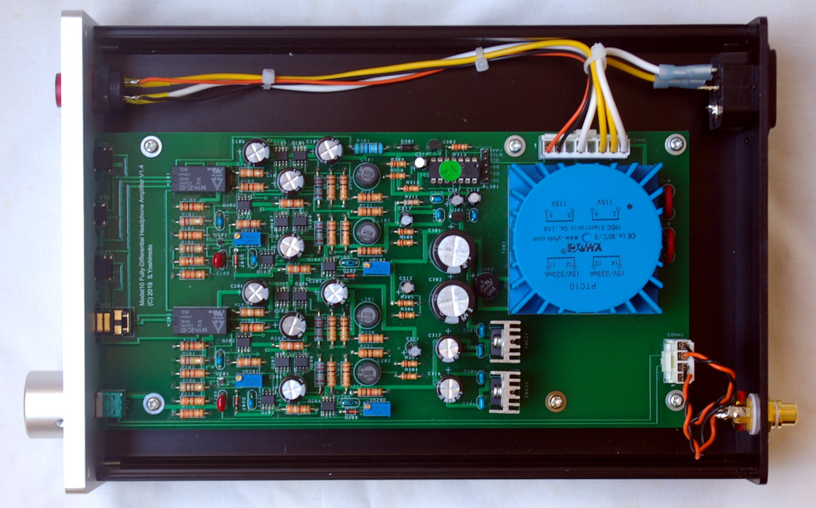
Almost all circuits are mounted on one printed circuit board.
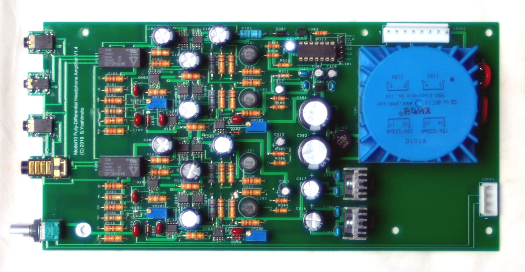
Below is a PDF file of the circuit diagram on the printed circuit board.
Model10 headphone amplifier board complete circuit diagram (.pdf)
| Balanced output | Unbalanced output | |
| Output power | 3.5W/32ohms | 1W/32ohms |
| Gain | 14dB | 7dB |
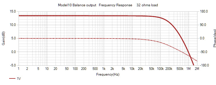
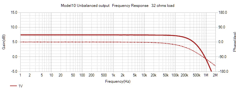
| Frequency Response | DC - 250kHz (-3dB) | |
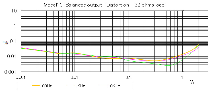
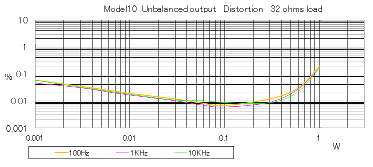
| Distortion at 100 mW | 0.01% or less | 0.01% or less |
| Noise(Uncorrected) | 48uV | 29uV |
| Noise(Hearing corrected) | 34uV | 17uV |
Balanced output
Unbalanced output
Balanced output
Unbalanced output
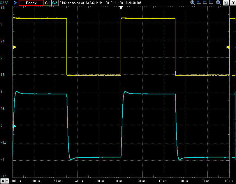
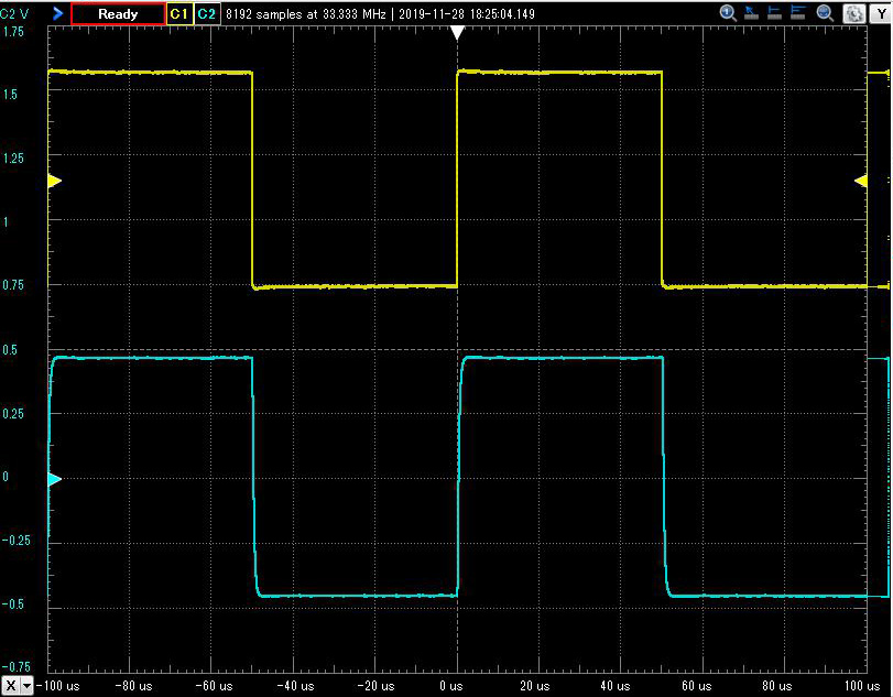
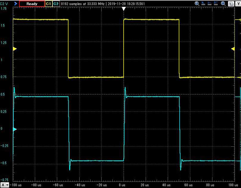
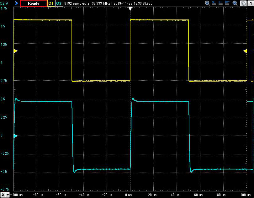
Balanced output 10KHz square wave response
The upper line is the input waveform and the lower line is the output waveform.
Click to enlarge.
 |
 |
 |
 |
| 32 ohms load | 32 ohms +0.001uF | 32 ohms +0.01uF | 32 ohms +0.1uF |
Unbalanced output 10KHz square wave response
The upper line is the input waveform and the lower line is the output waveform.
Click to enlarge.
 |
 |
 |
 |
| 32 ohms load | 32 ohms +0.001uF | 32 ohms +0.01uF | 32 ohms +0.1uF |
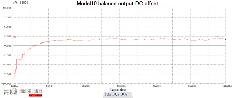
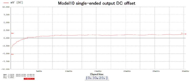
Since Model10 is a DC amplifier, the offset voltage generated at the output
must be suppressed.
A low offset voltage is realized by adopting dual elements for all amplification stages and fixing 0V by common mode feedback.
The figure below shows the offset voltage measurement results from power-on to 30 minutes.